Exciting news from Stanford Engineering!
Researchers have developed an ultrathin material, niobium phosphide, that conducts electricity better than copper in films just a few atoms thick. This breakthrough could revolutionize nanoelectronics by enabling more energy-efficient and powerful computer chips.
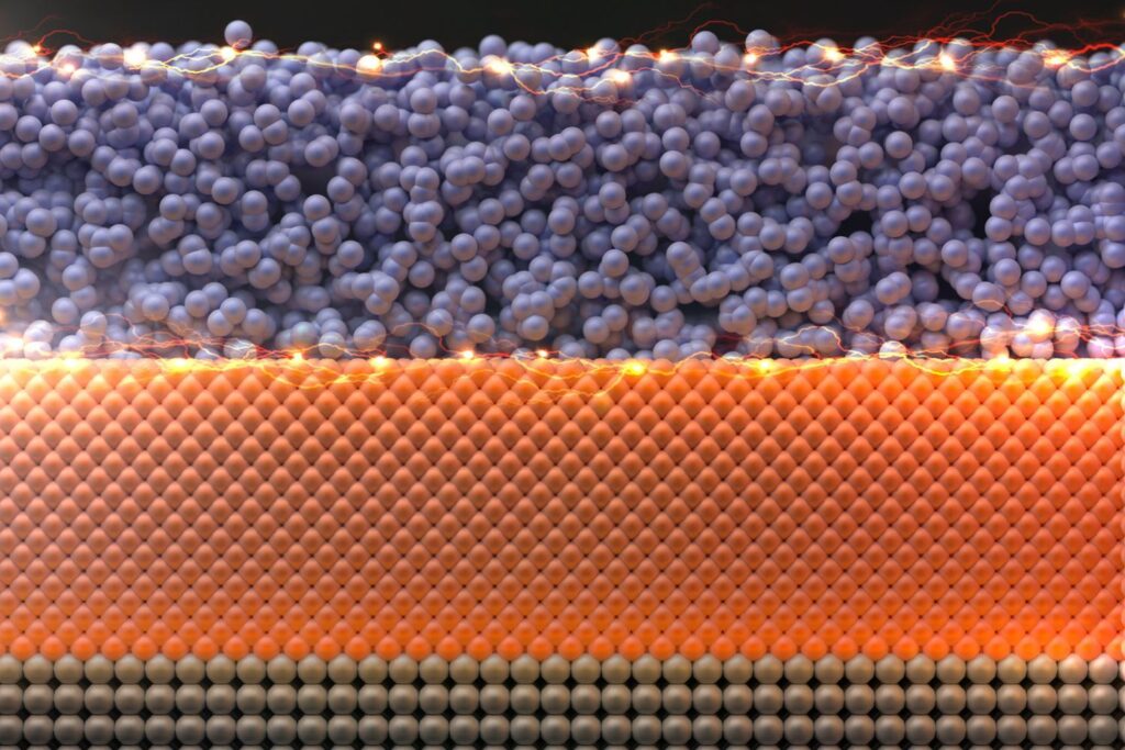
As computer chips get smaller and more complex, traditional metal wires like copper have become a bottleneck. They lose efficiency as they get thinner, limiting performance and energy savings. But niobium phosphide flips the script, it actually becomes a better conductor as it gets thinner, thanks to its unique properties as a topological semimetal.
What Makes This Discovery Even More Promising?
- Conducts better than copper at film thicknesses below 5 nanometers.
- Can be deposited at low temperatures (400°C), compatible with modern chip fabrication.
- Opens the door to using non-crystalline materials for nanoscale electronics, overcoming challenges faced by traditional crystalline structures.
This could improve the energy efficiency of future chips,” says Asir intisar Khan, first author of the study. “Even small gains add up when you think about the massive data centers powering our digital world.”
The Implications are huges:
- Faster, more efficient signals in ultrathin wires.
- Reduced energy consumption in electronics.
- A new class of materials, topological semimetals, that could pave the way for next-gen conductors.
While niobium phosphide isn’t set to replace copper entirely just yet, it’s a game-changer for the thinnest connections in nanoelectronics. The Stanford team is already exploring similar materials to push performance even further.
This research, published in Science, bridges cutting-edge physics with real-world applications. It’s a shining example of how innovation in materials science can address some of the biggest challenges in technology today, power efficiency, miniaturization and sustainability.
Congrats to the Stanford team for this incredible leap forward!
Source: https://lnkd.in/gwQm27Ex